Starting my blog,
As I approach nearly 20 years of working as a packaging development engineer, I wanted to compile all the knowledge, skills, and experiences I have gained and learned about packaging in one place. Looking back over the past two decades, there have been significant technological advancements in the packaging field, and recently, as the role of packaging in the semiconductor industry has become increasingly important, there has been a surge of interest and an accelerated pace of related technology development.
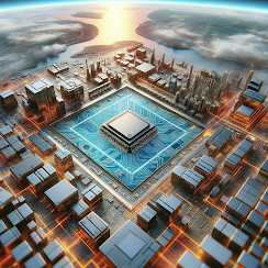
The most significant change is that the concept and scope of packaging have greatly expanded. Previously, there was a clear boundary between the front end, known as the fab process, and the back end, referred to as the packaging and assembly processes. However, the packaging concept has now extended to the back-end-of-line (BEOL) of the fab process. Until now, we have been increasing the chip's integration density according to Moore's Law; however, we have begun to reach the limits of increasing density on a single chip. By stacking multiple chips through packaging, the importance of packaging technology has never been greater in enhancing device integration density. Moreover, traditional packaging processes have been perceived as having lower technical difficulty compared to semiconductor chip manufacturing processes. However, as the importance of packaging grows, packaging technology is also advancing in sophistication.
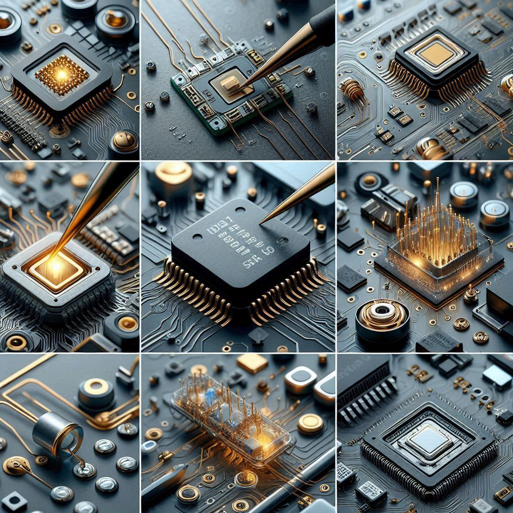
Packaging can be categorized into several fields depending on the type of device being packaged. When we refer to electronic packaging, we are generally talking about the assembly of semiconductor chips. Other categories include MEMS packaging for MEMS devices, photonics packaging for photonic devices, power electronics packaging for chips that handle high voltage and high current, and packaging in the biomedical field.
In this blog, I will aim to cover all these packaging areas as much as possible. Regardless of the application field, I will also address common packaging technologies, such as chip bonding and joining techniques that are widely used. I will periodically update the content to keep up with the latest trends in packaging technology. I wish for progress for those engaged in the research, development, and production of packaging, as well as for those who need packaging technology. To begin this blog, I will start with photonics device packaging, which has been researched for a long time and is currently seeing significant research and development activity.
Looking forward to the articles to come 🙌
ReplyDelete