Photonic packaging involves assembling and integrating optical components into a functional optical system, enabling the manipulation and transmission of light for communication and information processing. This process is analogous to the electronic packaging of semiconductor chips, where individual components are encapsulated to protect them from external influences and to facilitate connections with other electronic components.
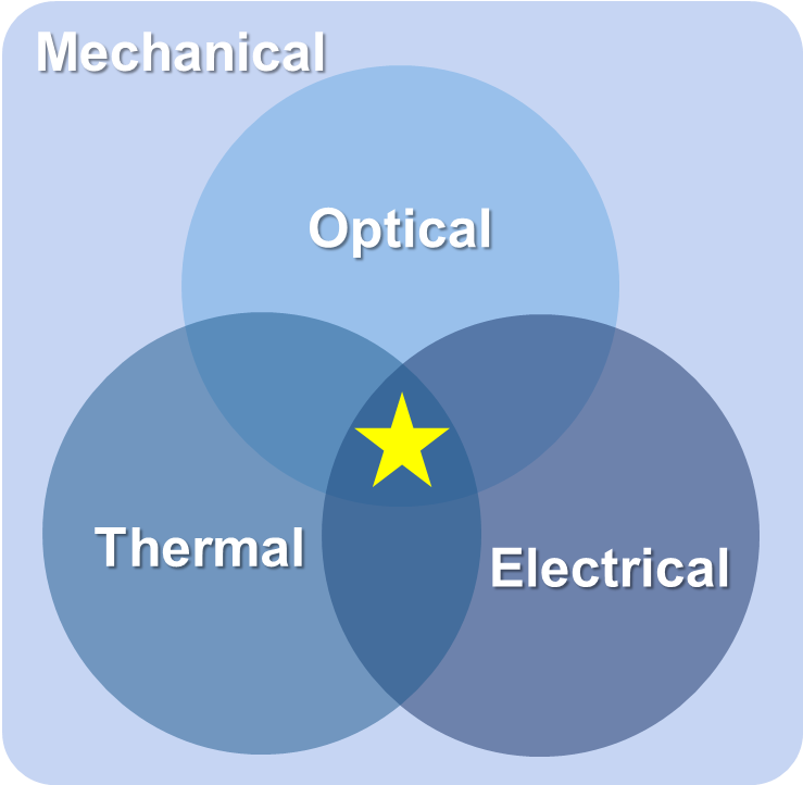
Photonic packaging is based on the same concept as electronic packaging, providing mechanical structures to protect optical devices from external physical and chemical environments such as dust, moisture, and vibration. Integrating various optical components into a single package ensures stable operation even in diverse operating environments. Additionally, since optical devices need to connect with multiple electronic components, the packaging can include wiring and connectors for electrical signal transmission and cooling systems to effectively manage heat generated within the package for stable device operation. Packaged optoelectronic devices are utilized in various fields such as communications, sensors, imaging, medicine, space, and defence technology.
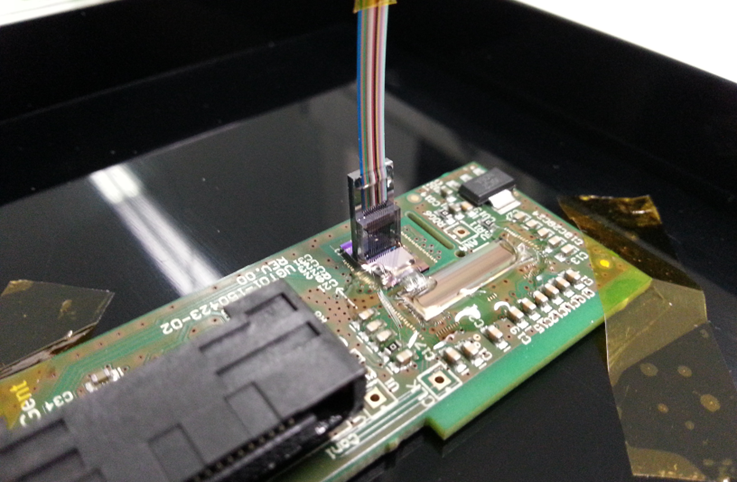
The core components of photonic packaging systems include photonic integrated circuit chips, electrical or optical interposers, fiber arrays, lenses, filters, laser diodes, photodiodes, amplifiers, substrates, and mechanical housings. These components, which are commonly used in electronic packaging, are combined with various optical devices and components to create functional photonic systems. The precise alignment of optical fibers and components within the package is a critical aspect of photonic packaging, and it will introduce the optical alignment techniques and components employed to achieve this.
Through the articles on this blog, I aim to share fundamental knowledge, experiences, and insights necessary for graduate students, researchers in research institutes, and development engineers in industries seeking to initiate product production in semiconductor packaging and silicon photonics packaging. Additionally, I will strive to contribute to advancing related technologies by studying the latest packaging technologies.
Comments
Post a Comment