- Working principle
Si photonics chips process data using light(1.3 μm (O-band) and 1.55 μm (C-band) regions) as a medium. To generate optical signals, an external laser or an integrated light source sends light into the waveguides within the chip. An optical modulator adjusts the intensity, phase, or frequency of the light sent through the waveguide based on electrical signals, encoding the data and modulating the signal. The modulated optical signal then travels through the waveguide within the chip or is transmitted to an external optical fiber. An optical detector converts the received optical signal back into an electrical signal to recover the data.
- Characteristics and Advantages of Si Photonics
Si photonics chips offer the following characteristics and benefits:
High-Speed Data Transmission: Light travels much faster than electrons and provides a wide bandwidth, supporting hundreds of gigabits per second (Gbps) or more transmission speeds.
Low Power Consumption: Using optical signals instead of electrical signals reduces power loss and heat generation.
Miniaturization: Leveraging silicon’s properties, optical components can be fabricated at the micron scale, resulting in compact chip sizes.
Cost Efficiency: By utilizing existing semiconductor manufacturing processes, production costs are reduced during mass fabrication.
Compatibility: Easy integration with electronic circuits enables the design of hybrid systems.
A notable drawback is that silicon struggles to generate light directly, requiring integration processes such as external light sources or bonding with III-V semiconductors to address this limitation.
- Applications
Si photonics chips are utilized across various industries and technology sectors:
Data Centers and Telecommunications: Employed as optical transceivers in fiber-optic networks for high-speed data transmission, playing a critical role in cloud computing and 5G communications.
Sensing: Used in LiDAR (light-based distance measurement) systems for environmental perception in autonomous vehicles and in biosensors for health monitoring.
Computing: Overcoming the limitations of traditional electronic chips, optical computing enhances the speed and efficiency of artificial intelligence (AI) and high-performance computing (HPC).
Medical and Biotechnology: Implemented in Lab-on-a-Chip devices to create miniaturized diagnostic systems, enabling rapid biochemical analysis.
Military and Aerospace: Due to their high reliability and lightweight properties, they are used for communication and sensing in aerospace and defence applications.)
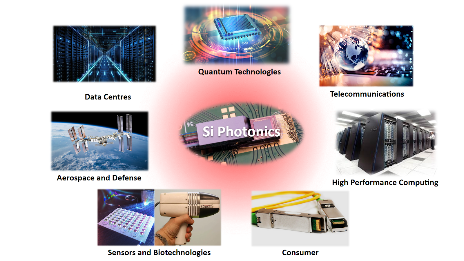
<Applications for Si Photonics>
Si photonic chips possess remarkable potential, but several challenges need to be addressed. Silicon has characteristics that make it difficult to generate efficient light source lasers, so hybrid integration packaging technology with III-V semiconductors is continuously being developed. To effectively manage the heat generated during the high-density integration process, packaging with cooling devices is essential. Additionally, optical components require precise alignment and fabrication, which impacts process costs and yield. Current research is focused on integrating light sources fully onto a single chip or introducing new materials and design approaches, such as quantum dot lasers and 2D materials like graphene, to address these issues.
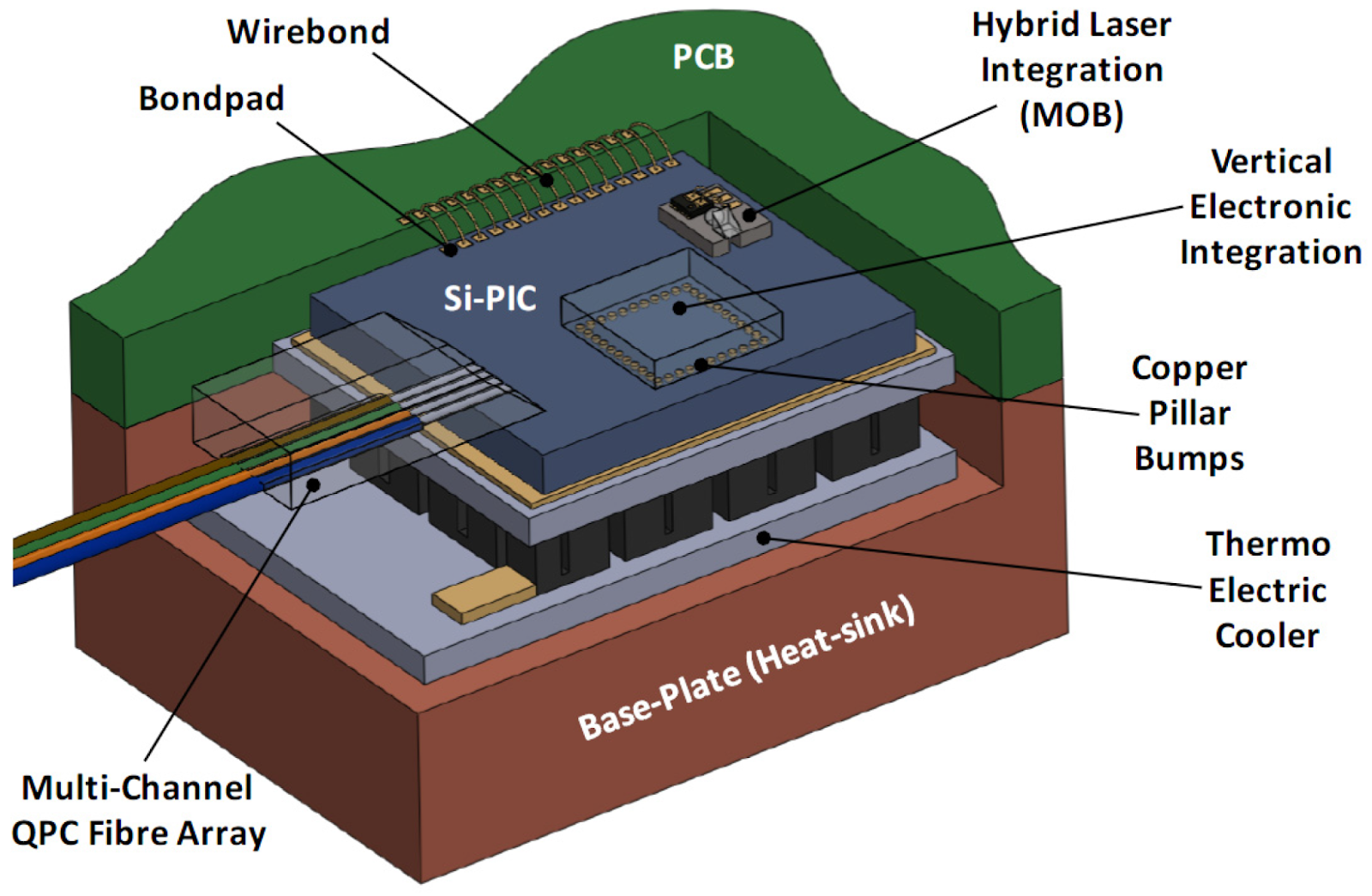
<The concept of hybrid integration packaging technology with III-V semiconductors>
Comments
Post a Comment